In today’s high-stakes electronics manufacturing, Printed Circuit Boards (PCBs) must be flawless. With rising complexities—from ultra-fine components to densely packed assemblies—traditional inspection methods are no longer sufficient. Intelgic’s next-generation PCB Board Inspection for Component Verification uses a powerful Machine Vision System and delivers Micron-Level Defect Detection, ensuring speed, accuracy, and scale that modern production demands.
Why PCB Component Verification Needs Innovation
Manual inspection is increasingly unreliable due to:
- High component density, with hundreds of miniaturized parts per board.
- Micro-scale defects—like lifted pins or solder cracks—often under 10 microns and invisible to the naked eye.
- Real-time requirements, where inspection must keep pace with automated SMT lines.
To eliminate human error and sustain quality, manufacturers require smart, automated solutions.
Intelgic’s Intelligent PCB Inspection Solution
Intelgic offers a turnkey platform for high-throughput, precision inspection:
Component Verification & Counting
AI-powered cameras verify component presence, correct orientation, and alignment to the BOM or CAD template. Missing or misplaced parts trigger real-time alerts.
Micron-Level Defect Detection
Thanks to ultra-high-resolution imaging and advanced AI algorithms, defects smaller than a few microns—such as micro-cracks, lifted solder joints, or component scratches—are detected reliably.
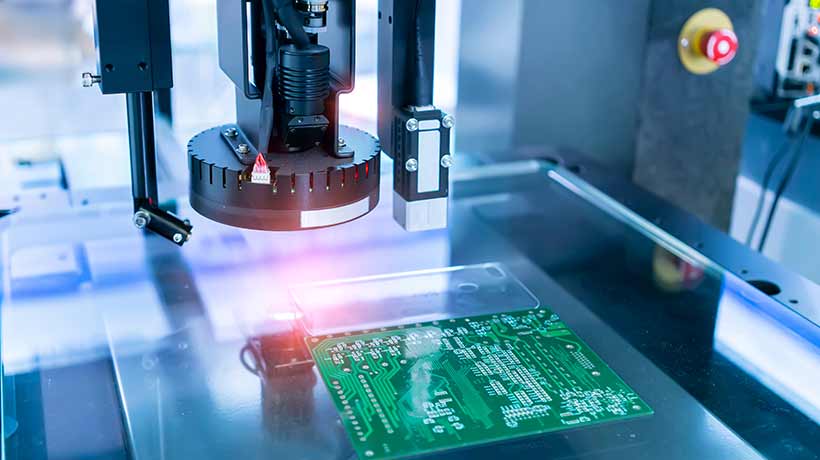
Robotic Imaging Systems
Inspect large, complex boards with precision. Cameras mounted on 3-axis robotic rails scan boards using X, Y, Z motion for full coverage—even multi-layer or rigid-flex PCBs.
Adaptive Lighting
Intelgic’s lighting systems—coaxial, dome, red/blue/white spectrum—adjust dynamically to reflectivity and board textures, minimizing glare and maximizing defect visibility.
Live Vision AI Software
Visualize, override, and audit inspection results through an intuitive interface. Integrates seamlessly with MES systems for traceability and production control.
The Workflow in Action
- Set-Up & Calibration
Align robotic imaging system and image parameters; ensure lighting and focus are optimized. - Auto-Scanning
The machine vision camera sweeps across the board, capturing high-resolution tiles. - AI Analysis
Images undergo multi-layer AI analysis—verifying components, solder joints, and surface integrity. - Defect Flagging
Detected anomalies (even micron-scale) are flagged for review or automated rejection. - Report & Traceability
Defect summaries, annotated images, and timestamps are logged and integrated into MES/ERP systems.
Advantages Over Traditional Inspection
| Benefit | Impact |
| Speed & Throughput | Up to hundreds of PCBs per minute. |
| Accuracy | Micron-level detection, especially for micro defects. |
| Non-Contact & Safe | No risk of physical damage during inspection. |
| Adaptability | Rapid recipe switching for different board layouts. |
| Traceability | Complete audit records via Live Vision AI analytics. |
Industry Applications
- Consumer Electronics
Ensures flawless placement of tiny 0201 components and detects solder defects invisible to the human eye. - Automotive Electronics
ECUs and safety modules rely on defect-free, accurate placement—realizable only with AI-powered AOI. - Medical Devices & Aerospace
Defect-free, traceable PCBs are non-negotiable; Intelgic brings lab-level precision to production floors.
Best Practices for System Integration
- Schema-Driven Setup
Use design data (BOM, Gerber) to train AI models tailored to board components. - Lighting Calibration
Simulate reflectivity and board textures in situ to minimize false detections. - Recipe Management
Maintain inspection templates for rapid switching between board types. - Operator-Friendly Feedback
Use Live Vision logs to train personnel, refine thresholds, and reduce rework costs. - Analytics Loop
Feed inspection data into SPC tools to identify root causes and continuously drive process improvement.
The Future of PCB Inspection
Advanced trends shaping the domain:
- Ensemble Learning Models
Combine EfficientDet, YOLOv5, and others for robust defect detection across scales. - Edge-Based Models (e.g., PCBDet)
Efficient, fast inference on ARM architectures supporting in-line inspection. - Deep, Multi-Depth Learning Models
Multi-scale defect detection via CNN architectures like YOLOv5 variants for improved real-time precision. - AI-Assisted Fiducial & OCR Mapping
Use fiducial marking and OCR to align real-time imaging with board layouts and securely track PCBs.
Expert Insights
“Machine vision systems can inspect up to 300 PCBs per minute… detecting tiny misplacements that would escape human inspection.”
— Industry benchmarking analysis.
“Micron-level defect detection is no longer optional…it’s essential for modern PCB production.”
— Intelgic’s Smart AOI announcement.
By leveraging PCB Board Inspection for Component Verification through robust Machine Vision Systems and Micron-Level Defect Detection, manufacturers shift from reactive to predictive quality assurance. Intelgic’s robotics-integrated approach delivers unmatched precision, speed, and data-driven reliability—ensuring every PCB is manufactured to perfection before it moves forward.
————————————————————————————————–